← Semiconductors 101: a free course following the life of a chip
Semiconductors 101, unit 13
Doping: ion implant and annealing
Very pure silicon barely conducts. A chip needs "this small region conducts, the one next to it doesn't", so a tiny amount of other atoms has to go into the right places, at the right depth.
Goals
- Explain why pure silicon barely conducts, how n-type differs from p-type, and how n and p are laid out so a switch stays off until a voltage on its gate turns it on.
- Explain how an implanter drives atoms into silicon, what the energy and the dose each decide, and how photoresist blocks the places that shouldn't be implanted.
- Explain why the wafer is annealed afterwards, why a wrong implant can't be saved, and why the settings are checked before the run and the sheet resistance measured after.

Step by step
- Add a tiny amount of phosphorus or boron to the silicon (doping).
WhyAlmost none of pure silicon's electrons can jump the band gap, so it barely conducts; phosphorus adds electrons that move (n-type), boron leaves empty spots (p-type).
If notWithout doping, silicon barely conducts and makes no switch; doped but not laid out in opposite types like n, p, n, the entrance and exit are connected all the time and the switch can't turn off.
- First cover the places that shouldn't be implanted with resist, leaving openings.
WhyOnly some small regions should be implanted; ions that hit the resist stop inside it and never reach the silicon.
If notThe beam sweeps the whole wafer, so anything left uncovered gets doped too.
- Turn the atoms into ions and drive them into the silicon with an electric field (ion implantation).
WhyImplanting needs no high heat, so the resist survives, and how much goes in and how deep is precisely controlled.
If notEarly doping let atoms seep in inside a hot furnace, a temperature resist can't survive.
- Set the energy and the dose: energy decides how deep, dose how many.
WhyThe harder the ions are pushed, the deeper they go; the more atoms per small area, the better that region conducts.
If notWrong energy leaves atoms at the wrong depth, a wrong dose gives the wrong conductivity, and the wrong atom can swap n and p.
- Heat the wafer once after implanting (annealing).
WhyA single ion can knock more than a thousand silicon atoms out of place on its way in, and most implanted atoms sit in the wrong spots, not yet conducting.
If notToo little and the region doesn't conduct well enough; too long and the atoms drift sideways and deeper, blurring the shape.
- Before the run, check atom, energy and dose one by one.
WhyA wrong implant looks exactly the same and is often found only at measurement, or even at electrical tests once the wafer is finished (at what voltage the transistors turn on, how much they leak).
If notThe atoms can't be picked back out; a wrong implant is usually put on hold for review and scrapped if it can't be used.
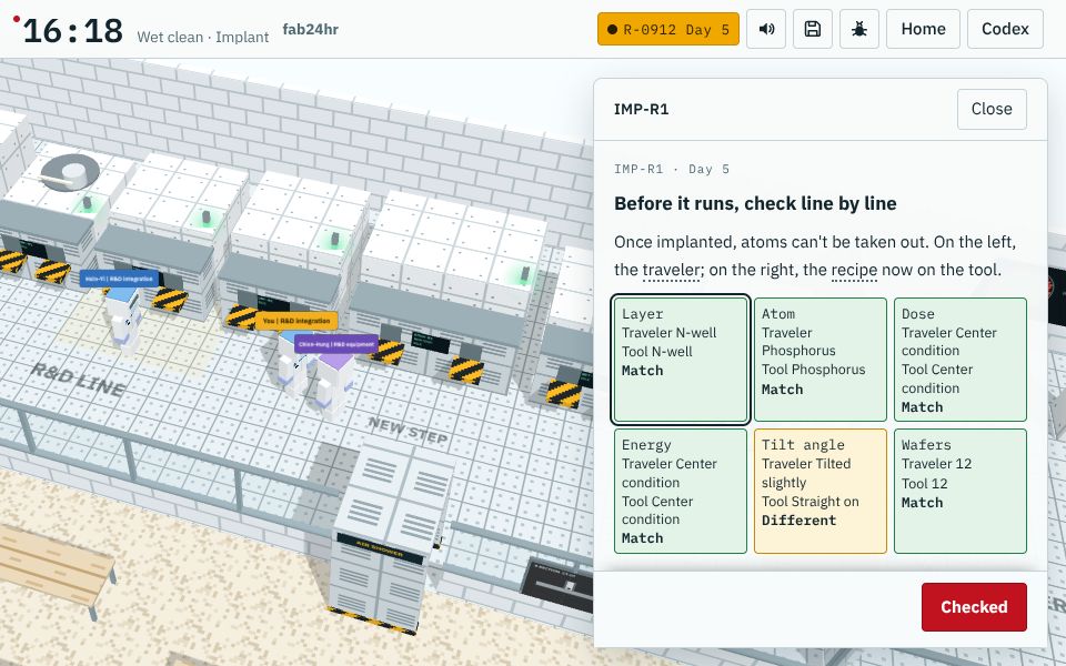
A screen from the game fab24hr; the tools, lot numbers and people are fictional. Play this part in the game → - Regularly implant a monitor wafer (one never shipped, kept to check the tool) and measure its sheet resistance after annealing.
WhyThe atoms can't be seen, so what is measured is how well the layer conducts; the tool's own count can drift.
If notIf the part that measures the beam current drifts, the tool stops at the wrong number and thinks the dose is exactly right; without a monitor wafer, no one notices.
What you adjust, what can go wrong
- Type of atom
ChangesPhosphorus (or arsenic) makes n-type; boron makes p-type.
If it is offThe wrong atom can even swap n-type and p-type.
- Energy
ChangesSets how deep the atoms go; typical depths are mostly between 10 nanometers and 1 micrometer.
If it is offWrong energy leaves the atoms at the wrong depth.
- Dose
ChangesHow many atoms go into each square centimeter, from about a hundred billion to ten million billion; the more, the better it conducts.
If it is offA wrong dose gives the wrong conductivity, and the switch's threshold and leakage shift with it.
- Anneal temperature and time
ChangesLets the jumbled silicon line up again, so the implanted atoms take their places and start to conduct.
If it is offToo little and too few atoms settle in, so it doesn't conduct enough; too long and the atoms drift sideways and deeper, blurring the shape.
Key ideas
Pure silicon barely conducts; a little added makes it n-type or p-type
A silicon atom's four outer electrons are like four hands, each holding a neighbor, so they are tied up and can't move. To move, an electron first has to jump a step called the band gap. Metals have no step, glass has a very high one, and silicon's is in between: at room temperature only about one electron for every few trillion silicon atoms gets over it, so pure silicon barely conducts. Adding a tiny amount of other atoms on purpose is called doping. Add phosphorus, with five outer electrons, and one electron is left loosely held and moves easily: that's n-type. Add boron, with only three, and an empty spot is left (a hole); neighboring electrons step into it one after another, so the spot seems to move: that's p-type.
n, p, n back to back: the switch is off by default
In a common kind of transistor, the source and drain are n-type and the block under the middle is p-type. Where n meets p, current can only go one way; push the other way and it meets something like a wall. Going from source to drain means crossing two boundaries back to back, so whichever way you push, one wall blocks it, and the switch is off by default. Put a positive voltage on the gate and, through the insulating layer, it pulls electrons to the surface of the p-type silicon; a thin layer there starts behaving like n-type, like a temporary bridge, and current gets through. Take the voltage away and the bridge falls apart. The voltage it takes to lay the bridge is the threshold voltage; the more heavily the p-type block underneath is doped, the higher it is.
The other kind works the other way, so two wells and many implants
The other kind of transistor swaps n and p, so it's p, n, p, and it's on only when the gate voltage is low. Chips mostly pair the two kinds, one connecting the output to the power supply and one to ground, which is called CMOS; so the same silicon needs both a p-type and an n-type "base", called wells. The two wells, the layer that sets the threshold, and the source and drain of each kind of transistor are all implanted separately. Each new place usually first needs a new stencil printed in photoresist by litho: ions that hit the resist stop inside it, only the openings let them into the silicon, and anything left uncovered would be changed across the whole wafer. So one process flow often implants about ten times, or more.
Inside the implanter: charge, speed up, count while shooting
A gas containing boron or phosphorus first becomes charged ions in the ion source, because only then can an electric field push them. The field speeds them up into a thin beam, and the whole path is under vacuum so the ions don't hit air. The beam sweeps the whole wafer. Ions carry charge, so the arriving ions are a current: the tool measures it, multiplies by time, knows how much has gone in, and stops when it's enough. The energy decides how deep the atoms go; the dose is how many atoms go into each small area, and the more, the better it conducts. Resist can be used as a shield because implanting needs no high heat. Early doping let atoms seep in by themselves inside a hot furnace, which resist can't survive, and many fabs still call the furnace area the diffusion area.
Anneal afterwards, with just enough heat
A single ion driving into silicon can knock more than a thousand silicon atoms out of place, leaving the layer a jumble, and most implanted atoms sit in the wrong spots and don't conduct yet. So the wafer is annealed: heat lets the silicon line up again, and only once the atoms take the places of silicon atoms do they start to conduct. But the longer the heat, the more the atoms drift sideways and deeper and blur the shape, and the smaller the structures, the less of that they can take. So many anneals now heat one wafer at a time for just seconds, while some still bake a whole batch in a furnace. Every later heating, oxidation and film growth included, moves the atoms a little more, an account called the thermal budget that is planned from start to finish.
A wrong implant can't be picked out: check before, measure after
Implanted atoms can't be taken out, unlike litho, where a misprint can be washed off and printed again, and a wrongly implanted wafer looks exactly the same. Too much in the block underneath and the threshold rises and the switch is slow; too little and it doesn't shut tightly and leaks. This is often found only at measurement or even electrical tests, and the lot is usually stopped and assessed, and scrapped if it can't be used. So the most important check comes before the run: atom, energy and dose, one by one. After the run, a monitor wafer (one never shipped, kept to check the tool) is implanted regularly and its sheet resistance measured after annealing, to see how well that layer conducts; the tool's own count of the current can drift too, so both are looked at.
Common misconceptions
- People saySilicon for chips should be as pure as possible; any other atom in it is contamination.
- In factThe silicon really is purified first, until metal impurities are down to around one part in a billion. But pure silicon barely conducts and can't make a switch, so once the unwanted atoms are gone, a tiny amount of the wanted ones is added on purpose, in the places chosen for them. Foreign atoms either way; the difference is whether they are the right kind, in the right place, in the right amount.
- People sayMeasure after implanting, and fix it if it's wrong.
- In factAtoms can't be seen, so what is usually measured is the sheet resistance, how well that layer conducts: too few atoms and it reads high, too many and it reads low, and it only reads true after annealing has put the atoms to work. Even when a reading is off, the atoms can't be taken out; the lot is usually stopped and assessed, and scrapped if it can't be used. Measurement catches a tool slowly drifting; what actually stops a mistake is the check before the run.
Look: machines to take apart
 Ion implanter
Read
- What is doping? How n-type and p-type silicon make a switch that's normally off
- What is ion implantation, and how does a fab shoot atoms into silicon?
Play
Play a shift as an implant process engineer: the atom, the energy and the dose are yours →
Think
- A wrongly implanted wafer looks exactly like a good one and may not be caught for a long time. If you were the one checking line by line before the lots go in, how would you make sure you don't miss a line? Who should check it again with you?
- An anneal has to be hot enough, but not too long. When "a bit more is safer" and "too much does harm" are both true, how would you decide where to stop?
Teaching materials: slides
The key ideas, diagram, machines and questions of this unit as a slide deck, ready to project or to put into your own handouts.
Download slides (PPTX)293 KBDownload slides (PDF)335 KB
Free to use in class and for non-commercial teaching. Please credit fab24hr. Do not sell it or present it as your own work. Spot a mistake? Report it
Cite this article"Semiconductors 101, unit 13:Doping: ion implant and annealing" fab24hr, updated . https://fab24hr.com/en/learn/doping/