← Semiconductors 101: a free course following the life of a chip
Semiconductors 101, unit 14
Wiring and polishing: CMP and layer upon layer of metal
Transistors are only useful once layers of metal wiring connect them. How the wiring is dug, filled with copper and polished flat decides whether current gets through, and how fast the chip runs.
Goals
- Explain why a chip is like a building: transistors at the bottom, layer upon layer of wiring above, joined up and down by vias and contacts.
- Explain why copper is dug first and filled after (damascene), why a barrier layer goes in first, and why copper-touched tools and wafers are kept apart from the front end.
- Explain why CMP polishes flat, where it stops, what goes wrong with too little or too much, and why wiring is slowing chips down more and more.

Step by step
- Stack layer upon layer of wiring above the transistors, joining the layers with vias.
WhyEach switch's result has to reach other switches, and there are too many wires for one layer.
If notSwitches that aren't connected are of no use, however many there are.
- Lay down an insulating layer, then use litho and etch to dig trenches and holes in it.
WhyCopper is hard to dry etch into lines, so the insulator is etched instead and the copper filled in (damascene).
If notEtch the copper directly and the products stick to the surface and won't etch clean; a hole not etched to the bottom doesn't connect the layers.
- Line the trenches and holes with a very thin barrier layer, then a thin copper seed.
WhyCopper atoms wander; the barrier keeps the copper in and helps it stick, and the thin copper is the seed the plated copper grows from in the next step.
If notCopper that gets into the silicon makes transistors leak, and it may not show right away.
- Electroplate, so copper fills the trenches and holes from the bottom up.
WhyAdditives in the plating bath make the bottom of a hole grow faster than its mouth.
If notIf the mouth closes first, a gap is left inside; current has trouble getting through, and in bad cases the connection breaks.
- Polish off the copper and barrier outside the trenches with CMP, stopping a little after the insulator shows.
WhyThe extra copper joins every wire into one sheet; the tool can't see the face, so a turn in motor force or reflected light tells it when it's there.
If notToo little and copper left between wires shorts them; too much and the wires thin and their resistance rises.
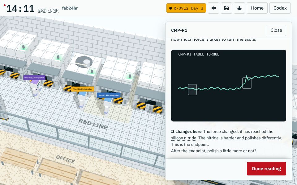
A screen from the game fab24hr; the tools, lot numbers and people are fictional. Play this part in the game → - Clean off the slurry particles right after polishing.
WhyA polished surface is covered in slurry, particles and debris from polishing.
If notAny particles left behind become defects in the next layer.
- Seal the top of the copper with a very thin protective film, then go back to the first step for the next layer.
WhyThe barrier wraps only the bottom and sides of the copper, so the top has to be sealed too.
If notCopper would work its way up into the insulator of the layer above.
What you adjust, what can go wrong
- Plating additives
ChangesMake the bottom of a hole grow faster than its mouth, so copper fills it from the bottom up.
If it is offIf the mouth closes first, a gap is left inside; current has trouble getting through, and in bad cases the connection breaks.
- Pressure and speed
ChangesThe harder you press and the faster it spins, the faster it polishes.
If it is offSet it differently from usual and the polishing speed changes with it; in the same time, it can remove too little or too much.
- Where to stop: endpoint and overpolish
ChangesA turn in motor force or reflected light means it has got there; the tool then polishes a little more as set to clear residue.
If it is offToo little and neighboring lines can connect; too much and lines thin, resistance rises, and wide lines sink in the middle.
- Slurry
ChangesSoftens a thin top layer so the pad and fine particles can take it away with a light touch.
If it is offIf the supply goes wrong, a larger hard bit can get caught between wafer and pad and drag a scratch.
- Pad and conditioner
ChangesThe conditioner scrapes the pad with tiny diamonds to keep it rough.
If it is offAs the pad wears it gets smooth, and the same time removes less and less.
Key ideas
A chip is like a building: wires, vias, contacts
At the bottom of a chip are the transistors, made in the silicon. The result from each switch is the voltage on a wire, high or low, and it has to reach other switches. There are too many wires for one layer, so they are stacked upward, more than ten layers in the most advanced chips. Metal lines running sideways within a layer are the wires, like corridors; tiny vertical holes connecting the wires of two layers are vias, like stairways; the holes at the very bottom that reach down to the transistors are contacts, often filled with a metal such as tungsten rather than copper. Fabs call the wiring part the back end of line, which is not the back end of test and assembly the industry talks about.
Copper is hard to etch, so dig first and fill after (damascene)
Wiring used to be mostly aluminum: cover the whole wafer, print the pattern, dry etch away what isn't wanted. Then came copper, because at the same size its resistance is only a little over 60% of aluminum's, and it holds up better than aluminum when a lot of current flows. But dry etching works by turning the surface into a gas that is pumped away, and copper's reaction products don't easily become a gas at temperatures the chip can take; they stick to the surface and the etch doesn't come out clean. So it's done the other way round: if you can't etch the copper, etch the insulator, dig the trenches and holes, fill in the copper and polish off the excess. This is damascene; filling the trenches and holes in one go is dual damascene. A hole not etched all the way down doesn't connect the layers; one etched too far damages the layer below.
Copper wanders: lock it in, and keep copper apart
Copper atoms wander. In the insulator, they make it insulate less well; in the silicon, even a little makes transistors leak, and it may not show right away. So before copper goes in, a very thin barrier layer lines the bottoms and walls of the trenches and holes, keeping the copper in and helping it stick; after polishing, a protective film seals the top. Front-end wafers still face very hot steps, and a trace of copper picked up along the way is driven into the silicon by the heat, possibly affecting the whole furnace load. So copper steps are done in a separate area or on dedicated tools, wafers that have had copper don't go back to the front end, and wafer boxes and handling equipment are kept separate too.
Electroplating fills the copper; CMP polishes off the rest and flattens
After the barrier comes a very thin layer of copper as a seed. The wafer goes into a plating bath with a current on, and copper grows from the seed; additives make the bottom of a hole grow faster than its mouth, so it fills from the bottom up, and if the mouth closes over first, a gap is left inside and current has trouble getting through. The copper also covers the surface outside the trenches, joining every wire into one sheet, so CMP (chemical mechanical polishing) removes the copper and barrier outside the trenches. It also flattens the surface: each film follows the shape beneath it, height differences pile up, and the scanner's range of sharp focus is shallow, so an uneven surface prints blurry in places. The slurry softens the top layer and the pad takes the high spots off first, so it keeps getting flatter.
Where to stop, and how polishing is watched
The wafer faces down where the tool can't see it, so the tool judges by a signal: when the surface changes to another material, the motor's force and the reflected light both change. This is endpoint detection, and the tool often polishes a little more afterwards to clear residue, which is called overpolish. Too little and copper left between two wires shorts them; too much and the wires thin and their resistance rises, and wide lines sink in the middle (dishing). A polished wafer is scrubbed right away, since particles left behind become defects in the next layer. A hard particle caught underneath drags a scratch, and a worn pad gets smooth and polishes more slowly, so a monitor wafer (one never shipped, kept to check the tool) is run regularly to measure how much comes off.
Fine below, thick above; wiring slows chips more and more
The bottom layers connect neighboring switches: short distances and a huge number of wires, so they are the finest and densest. The upper layers carry signals to the far side of the chip and deliver power to every switch: long distances and large currents mean wide, thick wires, because a longer wire has more resistance and a thicker one less. A signal on a wire faces two hurdles. The thinner the wire, the higher its resistance; and two wires with insulator between them act like a small capacitor, so the closer they are, the more a change of voltage on one tugs at its neighbor, and the slower the voltage changes. Making transistors smaller usually makes them faster, but making wires thinner makes them slower, so the more advanced the chip, the more of a signal's delay comes from the wiring.
Common misconceptions
- People sayWith CMP, the more you polish, the better.
- In factWhat has to go is the height difference and the extra metal, not as much as possible: CMP often stops just as a certain layer below is exposed. Polish too much and the lines get thinner and their resistance goes up, and wide metal lines sink in the middle like a shallow dish, which is called dishing.
- People sayA chip's circuit is a single flat layer printed on silicon.
- In factA chip is like a building: transistors made in the silicon at the bottom, and layer upon layer of metal wiring above connecting them, more than ten layers in the most advanced chips. Every layer has a different shape and goes round the loop again, so a wafer returns to litho dozens of times.
Look: machines to take apart
 Chemical mechanical polishing
Read
- How is the wiring inside a chip made? Vias, copper, and why the trenches come first
- What is CMP, and why do wafers need to be polished flat?
Play
Play a shift as a CMP process engineer: deciding how much to polish and where to stop →
Think
- A polishing pad gets smoother with use, so the same time removes less and less. What does stopping for two hours to change the pad cost, and what does lengthening the polish time to get by cost? Who is affected either way?
- The film from the step before came out a little thicker, still within spec, and what CMP polishes off changes with it. Between the two steps, who should notice first, and who should speak up first?
Teaching materials: slides
The key ideas, diagram, machines and questions of this unit as a slide deck, ready to project or to put into your own handouts.
Download slides (PPTX)488 KBDownload slides (PDF)453 KB
Free to use in class and for non-commercial teaching. Please credit fab24hr. Do not sell it or present it as your own work. Spot a mistake? Report it
Cite this article"Semiconductors 101, unit 14:Wiring and polishing: CMP and layer upon layer of metal" fab24hr, updated . https://fab24hr.com/en/learn/interconnect/